 Juchip Semiconductor
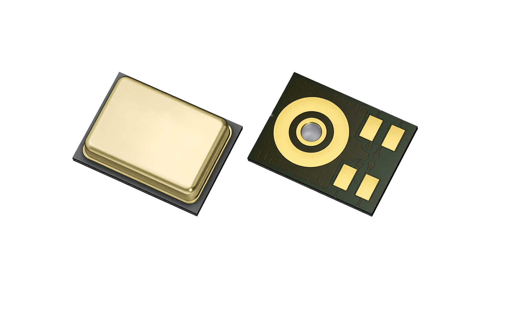
Bottom-Port Digital PDM Bone-Conduction Sensor (VPU)
JSV3526DT26GBP6
Bottom-Port Digital PDM Bone-Conduction Sensor (VPU)3.50×2.65×1.20mm · Bottom-port
A bottom-port digital PDM bone-conduction sensor (VPU) optimized for the wearer's own voice. It converts the acceleration of the surface it is mounted on rather than airborne sound pressure: pressed against the skull or ear canal, the wearer's voice reaches the sensing element through bone and tissue while ambient noise is largely rejected. Acoustic sensitivity loss (ASL) is 45 dB at 100 Hz and 40 dB at 1 kHz, keeping voice pickup usable in noise. A MEMS element plus PDM modulator outputs a single-bit PDM stream; an external clock selects sleep / low-power / standard, and the L/R pin sets which DATA channel is driven so two devices can share one DATA line.
- SNR (100 Hz–4 kHz, A-wt.)
- 63 dB(A)
- Sensitivity (Z, 1 kHz, 1 g)
- -20 dB
- Acoustic sensitivity loss
- 45 dB @100 Hz / 40 dB @1 kHz
- Peak frequency
- 8 kHz
Key Features
Six capabilities built for the voice chainWhy JSV3526DT26GBP6
Bone-borne voice, noise rejected
Converts surface acceleration, not air pressure: the wearer's voice travels through bone and tissue while ambient sound is rejected, so own-voice pickup survives noise and wind.
ASL 45 dB / 40 dB
Under a 94 dB SPL acoustic stimulus the output is 45 dB (100 Hz) and 40 dB (1 kHz) below a 1 g mechanical stimulus — a direct measure of airborne rejection.
Peak inside the voice band
The response peaks near 8 kHz (7.5–8.5 kHz), placing maximum sensitivity inside the bone-conducted voice band.
Single-bit PDM out
An integrated PDM modulator drives a single-bit stream clocked by external CLK — no external ADC or codec input stage needed.
Three clock-selected modes
Sleep (0–10 kHz), low-power (150–900 kHz, 320 µA @768 kHz) and standard (1.3–4.8 MHz, 750 µA @2.4 MHz) chosen by clock only; no mode register.
L/R channel, shared DATA
L/R tied to VDD drives DATA1, to GND drives DATA2 — two devices share one DATA line for left/right bone-conduction pickup.
Datasheet · Typical
Full SpecificationsSpecifications
Sensing & Acoustic
Sensing| Sensitivity (typ -20) | -22 / -20 / -18 dB |
|---|---|
| SNR | 63 dB(A) |
| ASL @100 Hz | 45 – 50 dB |
| ASL @1 kHz | 40 – 45 dB |
| Acceleration level | 4 g |
| Peak frequency | 8 kHz (7.5–8.5) |
Electrical & Timing
Electrical & Timing| Operating voltage VDD | 1.62 – 3.6 V |
|---|---|
| Standard current / clock | 750 μA @2.4 MHz |
| Low-power / clock | 320 μA @768 kHz |
| Sleep clock | 0 – 10 kHz |
| Clock duty | 40 / 50 / 60 % |
| TDV / TDZ | 40–100 ns / 5–20 ns |
| Load capacitance | ≤100 pF |
Mechanical, Reliability & Ordering
Mechanical & Reliability| Package | 3.50 × 2.65 × 1.20 mm, 6-pin LGA |
|---|---|
| Weight | < 0.03 g |
| Port | Bottom port (sealed sound hole required) |
| MSL | Class 1 (no pre-reflow bake) |
| ESD HBM | I/O ±3000 V |
| Operating / storage | -40~+85 °C / -40~+100 °C |
| Compliance | RoHS · halogen-free |
| Packing | Tape & reel · 5,000/reel |
Typical values at 25 C in the reference circuit; series production follows the official datasheet.
Pin Configuration
Pin DefinitionsPin Definitions
| Pin | Name | Description |
|---|---|---|
| 1 | GND | Ground |
| 2 | L/R | Channel select (VDD=DATA1, GND=DATA2) |
| 3 | GND | Ground |
| 4 | DATA | PDM data out |
| 5 | CLK | Clock input |
| 6 | VDD | Supply 1.62–3.6 V |
Ground all GND pins; place a 0.1 µF bypass close to VDD; keep CLK and DATA traces short and away from switching supplies and Class-D outputs (≤100 pF load); set opposing L/R levels when two devices share one DATA line. Values are taken from the engineering-evaluation datasheet; production parts follow the released datasheet and measurement.
Applications
Typical Applications & PairingWhere It Fits
Ordering & Packaging
Ordering & PackagingHow to Buy
- Packaging
- Tape & Reel5,000 pcs/reel
- Status
- Engineering samplesFinal spec per released datasheet
- Samples / Quote
- Request via inquiryFAE reply in 1 business day
Related Parts
Related Parts on the Same PlatformYou May Also Evaluate
Put this part into your next device
FAE support covers cavity review, reference circuits and dual-mic array references - reply within one business day.
Request Samples & Reference Design