 Juchip Semiconductor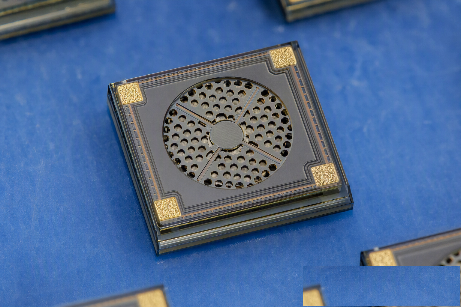
Capacitive MEMS Microphone Die
HJT1280A
Capacitive MEMS Microphone Die0.6×0.6×0.4 mm (die) · Top-port
An ultra-small capacitive MEMS microphone die: 0.6 × 0.6 × 0.4 mm with high static capacitance, low parasitics and a flat 50 Hz–10 kHz response. Au top metallization supports wire bonding; compatible with high-temperature reflow and COB processes — the sensing element for cost-driven in-house analog/digital mic modules. Delivered as wafer, 100% wafer-level tested. Delivered as wafer for module-level packaging.
- Die size
- 0.6 × 0.6 × 0.4 mm
- Static capacitance
- 0.45 pF
- Bias voltage
- 13 V
- Frequency response
- 50 Hz–10 kHz
Key Features
Six capabilities built for the voice chainWhy HJT1280A
Ultra-small footprint
0.6 × 0.6 × 0.4 mm die for the smallest acoustic cavities and highest board density.
High consistency
MEMS/semiconductor batch fabrication with 100% wafer-level test for consistency and repeatability.
Robust structure
Perforated rigid backplate, anti-stiction bumps, flexible membrane and back cavity — no degradation across wide temperature and humidity.
Process friendly
Au pads for wire bonding; 260 °C ×4 reflow (J-STD-020-C), SMT/SMD compatible.
Volume cost advantage
Batch MEMS/semiconductor fabrication with high die-per-wafer density — the chip sets the floor of your module BOM.
Environmental resilience
-40 ~ +100 °C operating range with long-term sensitivity stability across temperature and humidity; 260 °C ×4 reflow capable.
Datasheet · Typical
Full SpecificationsSpecifications
Electrical
Electrical| Static capacitance | 0.33 / 0.45 / 0.57 pF |
|---|---|
| Operating bias | 13 V |
| Test conditions | 23 ±5 °C / 45 ±15 % RH |
Absolute Maximum Ratings
Abs Max| Operating temperature | -40 ~ +100 °C |
|---|---|
| Storage temperature | -40 ~ +125 °C |
| Solder & reflow | 260 °C, 4 cycles (J-STD-020-C) |
Outline & Pads
Outline| Die size | 0.6 × 0.6 mm |
|---|---|
| Thickness | 400 µm |
| Pad size | 90 × 90 µm |
| Scribe line | 65 µm |
| Pad coordinates | V_out (80,520) · V_bias (520,520) · logo (520,80) · NC (80,80) µm |
Quality & Compliance
Quality| Test | 100% wafer-level test |
|---|---|
| Environmental | RoHS / REACH / halogen-free |
| Delivery | Wafer |
Typical values at 25 C in the reference circuit; series production follows the official datasheet.
Pin Configuration
Pin DefinitionsPin Definitions
| Pin | Name | Description |
|---|---|---|
| 1 | V_out | Voltage output |
| 2 | V_bias | Bias |
| 3 | LOGO | Foundry logo pad |
| 4 | None | NC pad |
The sensor area contains fragile membrane/backplate microstructures: never touch mechanically, never wet, and never apply vacuum or high air pressure on either side. Account for condensation and die-bond/PCB stress in housing design — they shift sensitivity.
Ordering & Packaging
Ordering & PackagingHow to Buy
- Delivery
- Wafer / wafer ringPer-lot wafer delivery
- Back-end Support
- Bonding & packaging referencesASIC selection & acoustic cavity guides
- Samples
- Evaluation waferRequest via inquiry
Related Parts
Related Parts on the Same PlatformYou May Also Evaluate
Put this part into your next device
FAE support covers cavity review, reference circuits and dual-mic array references - reply within one business day.
Request Samples & Reference Design